How does NV diamond sensing work?
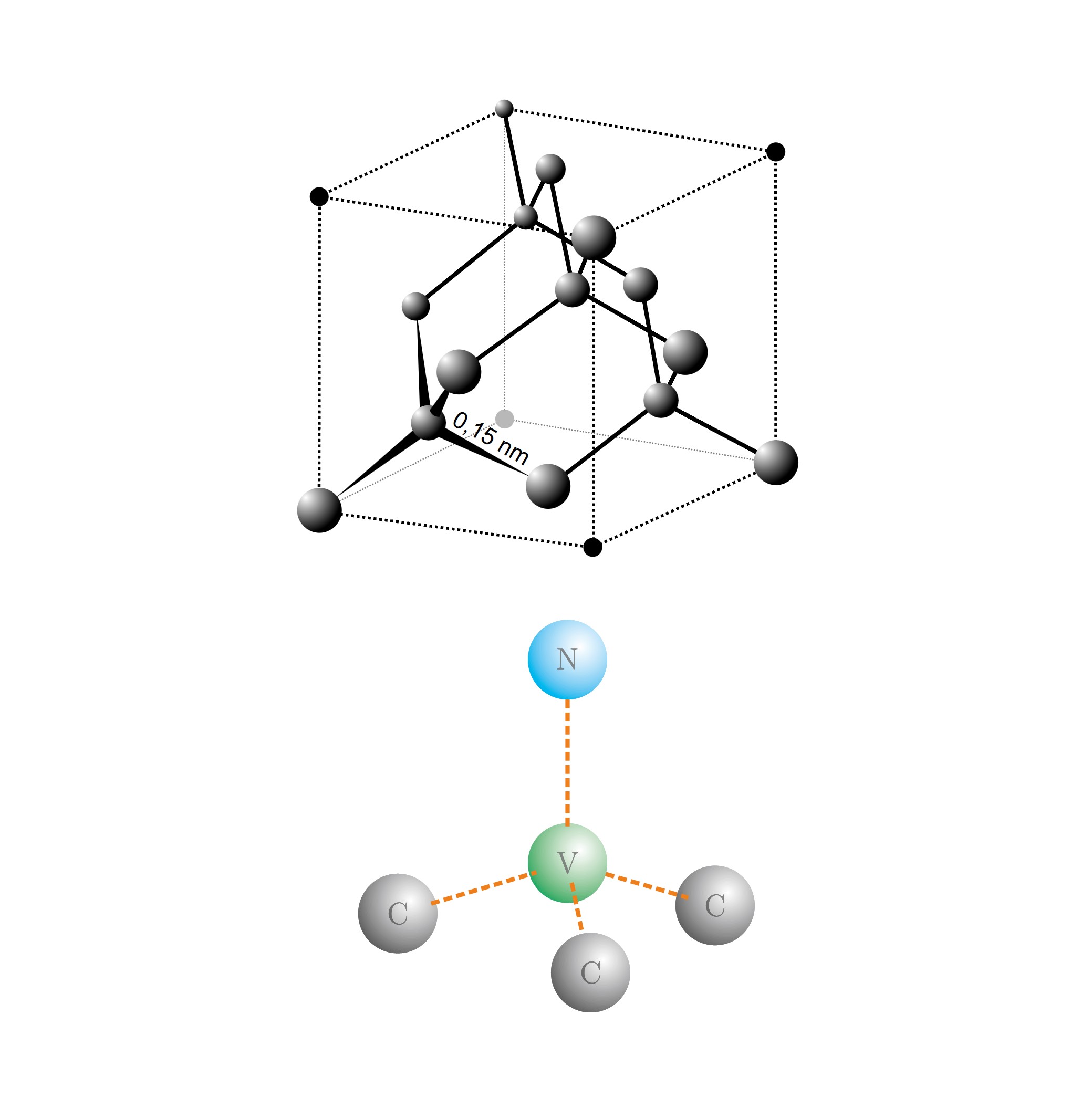
NV sensors use special Nitrogen-Vacancy centers (NV centers) in the diamond crystal that are extremely sensitive to magnetic fields, electrical and thermal influences. These quantum defects are optically excited by a green laser – the generated fluorescence depends on the local magnetic field and is read out via optical fiber.- Main advantages: contactless, galvanically isolated, robust against electromagnetic interference, measurement of DC and AC quantities as well as temperatures possible in extremely harsh environments
- Measurement is microwave-free (no heat input into the object, high safety in high-voltage applications)
- Isotope magnetic field measurement: Determines the magnitude |B| directly and spatially resolved
 Fig.: AMA Innovation Award 2023
Applications and Unique Selling Points
- Galvanically isolated high-voltage and current measurement
- Galvanically and thermally isolated highly accurate position sensing in the most difficult environments
- Magnetic field and eddy current cameras: visual representation of magnetic phenomena in real time
- Miniaturized sensor heads that can be used in medical catheters, between cables or in hard-to-reach industrial facilities
- Robust design, suitable for temperatures from −100 °C (probably lower) to +250 °C (probably higher) and aggressive chemicals or use in particle radiation
- Diverse applications from material testing, motor monitoring to research, life sciences and defense
More technical details and examples can be found in the official technology handout (PDF) by Quantum Technologies.
Benefits at a Glance
Contactless, galvanically and thermally isolated position, current and magnetic field measurement – robust, fast, at room temperature, without microwaves even in the most difficult atomic, chemical, biological, thermal environments.
How it works
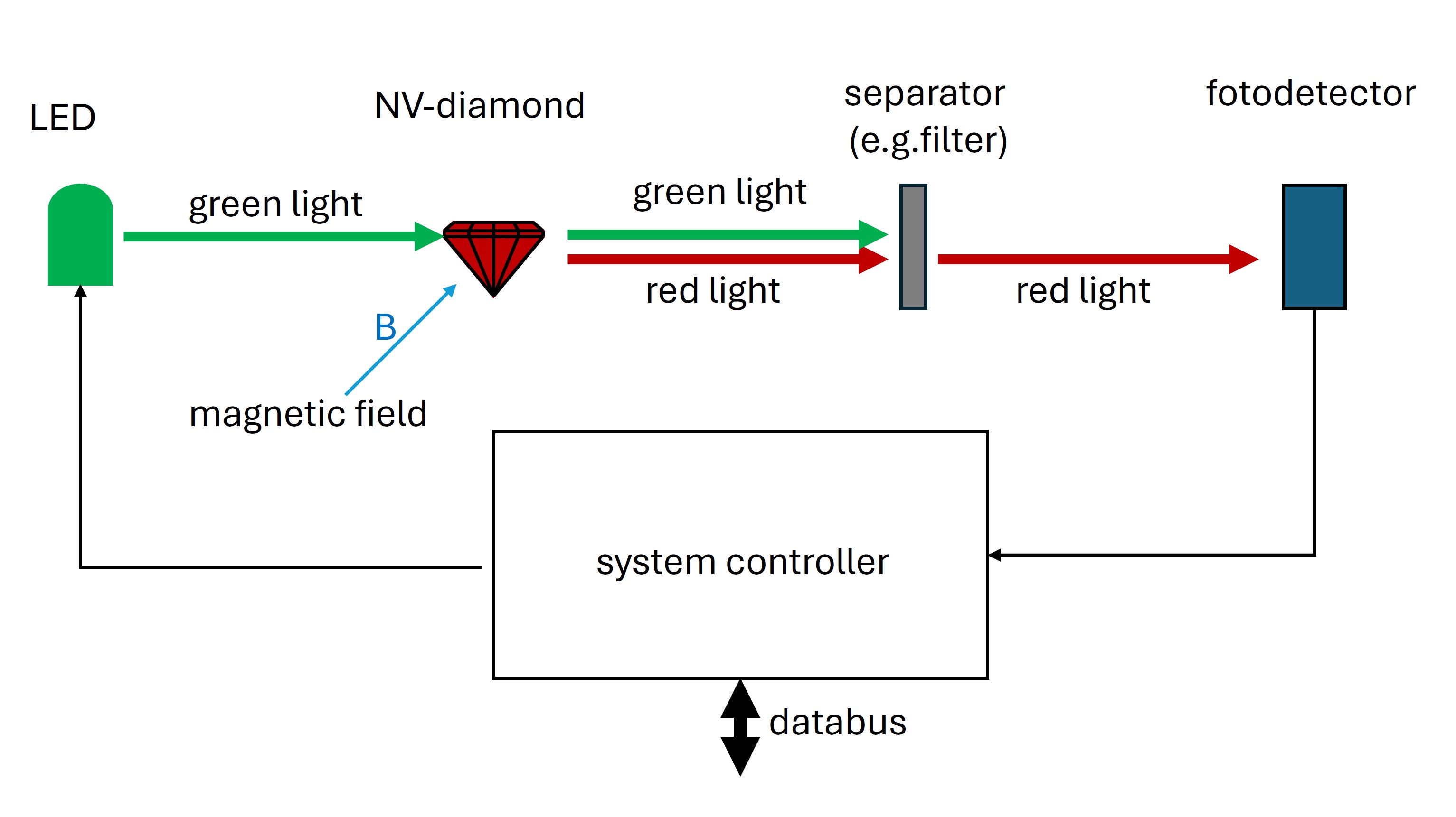
- The control unit causes a light source, e.g. an LED, to emit modulated green light.
- The green light excites NV centers in the diamond.
- The NV centers fluoresce red; the fluorescence intensity depends on the magnetic field B.
- The field-dependent red fluorescence is guided, e.g., via optical fiber to the evaluation unit.
- The field-dependent red fluorescence is typically separated there from the green light.
- The field-dependent red fluorescence is detected by a photodetector.
- The control unit detects the fluorescence change attributable to the magnetic field.
- The control unit derives one or more measured values from this – galvanically and thermally isolated from the measuring point.
Why microwave-free?
- Less complexity: no microwave generator or antenna required → more compact, cost-effective setup.
- Active EMC friendliness: no active microwave source, low interference.
- Passive EMC friendliness: no antenna effect due to missing microwave feed line.
- Energy efficient: lower power consumption, no self-heating.
- Robustness: fewer components → higher reliability and dependability.
- Cost advantage: simpler design, signal evaluation less complicated, packaging and integration faster and cheaper.
- Better suited for mass production, CMOS integration (low-power) and HV integration.
Applications
- Current measurement (e.g. HV batteries, inverters, DC link)
- Current density distribution (electrochemistry etc.)
- EMC diagnostics and magnetic field monitoring
- Magnetic field imaging (prototyping, QA, field distributions)
- Condition monitoring in machines and systems
- Position detection under the most difficult conditions
(medicine, industry, mining, drilling technology, defense, automotive, avionics) - Control and protection (e.g. wide-bandgap switches, optical fuses)
Material & Design Options
Basic types:
• Single-crystal diamond (sc-C): uniform lattice, NV axes defined, high sensitivity
• Polycrystalline (pc-C): many grains with different orientations; NV axes stochastically distributed over the volume; smooth measurement curves; use of the entire curve; bias magnetic field not necessary (= cost-effective)
Advantages and disadvantages:
• Single-crystal diamond (sc-C): uniform lattice, NV axes defined, high sensitivity
• oriented crystal: NV centers preferentially oriented (e.g. ⟨111⟩); no smooth curve; use of spikes for measurement; magnetic field must be stabilized.
• oriented crystal: NV centers stochastically distributed in four orientations in the crystal: four preferred orientations (difficult to useless). No smooth curve.
• oriented crystal: NV centers stochastically distributed in four orientations in the crystal: four preferred orientations (difficult to useless). No smooth curve.
• Polycrystalline (pc-C): many grains with different orientations; NV axes stochastically distributed over the volume; smooth measurement curves; use of the entire curve; bias magnetic field not necessary (= cost-effective)
| Variant | Advantages | Disadvantages |
|---|---|---|
| Single crystal, oriented and NV centers oriented | Vectorial measurement (3D), highest homogeneity/sensitivity, self-calibrating, good physical reproducibility, very low processability for series production | Expensive, complex manufacturing & orientation to microradian accuracy, sensitive to misalignment and fluctuations, only for niche markets |
| Single crystal, oriented and NV centers not oriented | Vectorial measurement (3D), high homogeneity/sensitivity, self-calibrating, good physical reproducibility, very low processability for series production | Expensive, complex manufacturing & orientation to microradian accuracy, sensitive to misalignment and fluctuations, only for niche markets |
| Polycrystalline, stochastic | Very robust, cost-effective, best mass integration option, isotropic scalar measurement, high NV density | Lower sensitivity, broader lines, self-calibrating systems possible, less suitable for precise vector analyses, very good for mass markets in areas where Hall, TMR, and GMR sensors do not work. |
| Polycrystalline, partially oriented | Very robust, cost-effective, best mass integration option, isotropic scalar measurement and anisotropic vectorial measurement possible with one substrate, high NV density | Lower sensitivity, broader lines, self-calibrating systems possible, suitable for simple vector analyses, very good for mass markets in areas where Hall, TMR, and GMR sensors do not work. |
Practical conclusion: For scalar, microwave-free current/magnetic field measurement in harsh HV environments, polycrystalline, stochastically distributed NV media are ideal (first choice for series production). For highest sensitivity and highly precise vector measurement, single-crystal, oriented NV media are suitable.
Performance Data & Integration
- Bandwidth: From DC to high frequency (design-dependent, up to several MHz)
- Response time: Down to the nanosecond range
- Isolation: e.g. optical fiber or other optical systems, high galvanic, thermal and radiation isolation
- Temperature range: −100 °C to +250 °C, radiation stable (e.g. fusion/X-ray environment)
- Form factors: Sensor elements in fiber-coupled variants possible with <50 µm diameter
- Form factors: Sensors (sensor element incl. electronics) from sugar cube to fingertip size, arrays, fiber-coupled variants
- Integration: CMOS/MOEMS-compatible, suitable for miniaturized systems and arrays
Advantages of NV Diamond Sensing (compact)
- Room temperature operation, no cryogenic need
- High isolation (galvanic, thermal, radiation)
- In current measurement contactless/shuntless → no line losses, no self-heating
- Metal-free actuation & readout – no arcing hazard, optimized for air gap/transformer/EMC
- Fast (ns), wide bandwidth (DC-MHz+)
- Mechanically, chemically robust (diamond)
- Low drift & tolerant in scalar measurements
- Miniaturizable
- for flexible array/camera concepts (from a few µm² up to several m²)
- also suitable for magnetic field distribution measurement on curved surfaces
- Long measurement paths from electronics to sensor element possible
- high distance sensitivity sensor element to sample
- Future-proof: proprietary IP, partners from industry & science
IP & Partners
- Intellectual property rights to key technologies and design variants lie with Quantum Technologies
- Strong contractual partnerships with academic and industrial R&D partners
- Long-term roadmap for industrial integration and technology leadership
Would you like a technical discussion, a sample, or a personal demo?
Contact us: info@quantumtechnologies.de | Tel.: +49 341 69764090
Contact us: info@quantumtechnologies.de | Tel.: +49 341 69764090