Facts at a glance
- Real-time imaging of magnetic fields and eddy currents (µT to mT range)
- Highest resolution through NV diamond sensor arrays
- Instant visualization of entire field distributions or current flow distributions – no single-point scanning
- Robust, fully optical and contactless measurement setup, insensitive to EMI, temperature & vibration
- Option for integration/use as an eddy current camera for eddy current imaging
- Ideal for laboratory, manufacturing, failure analysis, structural analysis and safety testing
- Request demo, trial and offer directly
Magnetic Field Camera
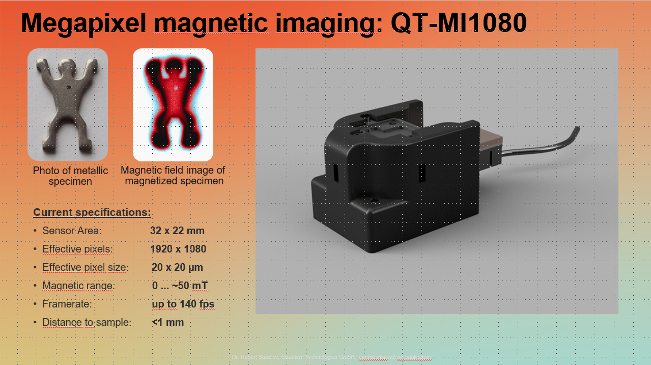
The NV Magnetic Field Camera uses a layer of disordered NV nanodiamonds in a carrier material for complete, imaging detection of magnetic field distributions in real time (range: µT to mT). The sensor arrays are optically read out via laser or LED and fluorescence – the magnetic field influences the red fluorescence of the NV nanodiamonds. This results in a fluorescence image, which is captured by a CCD camera and can, for example, be directly converted into a "magnetic field image."
Functionality:
The sensor head is fully optical, contactless, microwave-free and galvanically isolated. Field changes on the surface or inside the test object are displayed visually – in Full HD and up to 140Hz frame rate. With special cameras, massively higher frame rates (possibly up to 500kHz) are feasible. We are happy to test this with you. Defects, deviations or current flows and other local variations that modify magnetic fields immediately appear as local anomalies in the magnetic field image. For evaluation, the data can be directly compared with reference images, integrated into automated quality controls or AI-supported fault diagnoses. The high speed enables integration into mass production processes and other testing procedures.
Economic advantages:
- Immediate, non-destructive testing for cracks, cavities, inclusions and short circuits – defects are efficiently found, the cause can be directly identified from the image.
- Inline integration into manufacturing processes: real-time quality control, reduction of scrap and rework costs.
- Cost reduction in test benches and production lines – no contact-based sensor systems or long scanning times required.
- Universally applicable: for metals, electronic components, magnetic materials and complex structures, robust against environmental influences (EMI, temperature).
Eddy Current Camera
The Eddy Current Camera builds on the magnetic field camera in combination with a magnetic alternating field that specifically induces eddy currents in the material under investigation. These eddy currents generate a characteristic magnetic reaction field, which is recorded by the magnetic field camera as an image. The magnetic "reaction film" is compared with a reference image without a sample. In this way, the magnetic alternating fields used to generate the reaction fields can be removed from the images again.
Functionality and evaluation:
The technology makes it possible to immediately visualize defects such as cavities, cracks or inhomogeneities. Particularly interesting, however, is that local conductivity changes (e.g., broken fibers) can also be detected and visualized in non-conductive or complex composite materials such as carbon composites. The shape and extent of the defect are directly recognizable – cause analysis, process optimization and maintenance are massively simplified.
Economic advantages:
- Efficient, fast detection of material defects through direct imaging – reduces rework, scrap and production downtime.
- Inline inspection and automated defect detection possible – e.g., in composite manufacturing, battery production, turbine construction and automotive.
- Enables new testing approaches also for materials unsuitable for conventional eddy current methods.
- Improved root cause analysis, as the exact defect shape and location are traceable in the magnetic field film.
Industries & Application Areas: Economic Benefits
-
 Automotive & Aviation Industry:
Quality control of body and turbine components, carbon structures, safety-relevant components.
Huge savings on scrap, precise defect localization during production, reduction of costly recalls. -
 Energy Sector, Wind Power & Turbines:
Inspection of generators, blades and mechanical parts.
Immediate identification of microcracks/cavities increases reliability and service life, avoids downtime and repair costs. -
 Electronics & Semiconductor Manufacturing:
Inspection of circuit boards, chips and metal layers.
Early detection of short circuits, opens, voids – lowers testing costs and reduces rework. -
 Materials Research & Development:
Structural analysis of new materials, layer-based materials, development testing.
Faster innovation cycles through inline diagnostics and visualization of conductivity changes. -
 Medical Technology & Biotechnology:
Control and analysis of composite materials in prostheses or implants.
Quality assurance, prevention of material failure, innovation in measurement solutions for sensitive structures. -
 Construction Industry & Infrastructure:
Inspection of reinforced concrete, composite parts, elements for bridges and buildings.
Early detection of weak points, interface wear, crack detection, increased construction safety. -
 Defence & Security Applications:
Structural analysis of safety-critical components, tamper-proof detection.
Reduction of risks, rapid detection of manipulations, early recognition of material failure. -
 Research & Teaching:
Demonstration of physical effects, development of new diagnostic methods.
Realistic imaging and defect representation suitable for pupils and students.