Key Facts at a Glance
- Quantum-sensor PCB substrate with integrated NV diamond sensors
- Direct integration into high-frequency and microwave PCBs for spectrum analysis, magnetic field, and material diagnostics
- Self-adjusting sensor elements for maximum reproducibility and industrial mass production
- Area-wide measurement and visualization of magnetic fields, current density, and material properties at PCB level
- CMOS-compatible, modular, suitable for complex multi-sensor arrays
- Usable under extreme conditions: high voltage, high temperatures, aggressive chemicals, radiation environment
- Patented integration technologies and international protection rights
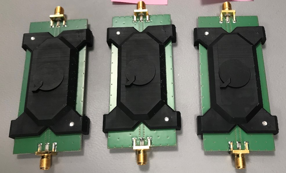
PCB Substrates for Special Applications
Structure & Functionality
The PCB substrates are based on an innovative combination of classical PCB technologies and embedded sensor elements.
Depending on the application, carrier materials – such as semiconductor wafers, microelectronic circuits, MOEMS, ceramics, glass, or composite layers – are anchored with diamond nanocrystals with NV centers through a radiation-hardened medium. These sensor elements self-align onto the relevant PCB areas (e.g., regions with waveguides, pads, structures for magnetic field or current measurement).
The sensors and sensor surfaces are optically pumpable and readable: pump light and evaluation fluorescence are guided through the transparent carrier material – contact-free, galvanically and thermally separated. This integration enables extremely precise, imaging measurement of magnetic, electrical, and structural properties on the PCB directly during operation, development, or testing.
Advantages of the Technology
- High Integration: Direct embedding into PCB, enables series production and scaling for complex multi-sensor systems.
- Self-adjustment: Patented curing and placement processes ensure optimal sensor alignment – minimal calibration effort, high accuracy (Cpk value).
- Multifunctionality: Combination of magnetic field measurement, high-frequency spectrum analysis, current and position diagnostics – all on one platform.
- Robustness: Extremely resistant to environmental influences, no metal contact required, no short-circuit risk, long lifetime.
- Industrializability: Compatible with modern PCB production lines, mass production possible.
- Cost Efficiency & Sustainability: Material savings, efficient inspection, minimized maintenance.
Industries & Application Areas: Economic Benefits
-
 Automotive & Aerospace Industry:
Precise magnetic field and current distribution measurement on PCB substrates in avionics systems and control boards. Increased operational safety of aircraft and automotive electronics, real-time fault detection, faster maintenance cycles, and avoidance of costly recalls. -
 Energy Sector, Wind Power & Turbines:
Condition monitoring and quality assurance of power electronics, generator PCBs, turbine controllers. Early detection of overheating, conductivity changes, and structural defects – more reliability, less downtime. -
 Electronics & Semiconductor Manufacturing:
Inline inspection of PCB controllers, high-frequency modules, and PCB arrays during production and development. Early detection of short circuits, delaminations, MRAM testing, minimal rejects, accelerated innovation cycles. -
 Materials Research & Development:
Structural analysis of new PCB composite materials, functional integration, high-end material testing. Rapid identification of conductivity, porosity, and tracking problems, optimized prototyping phases. -
 Medical Technology & Biotechnology:
Quality assurance of high-frequency boards and sensor arrays in medical measuring devices, implantable sensors. Error-free performance and environmental tolerance in critical applications such as diagnostics and monitoring. -
 Construction Industry & Infrastructure:
Monitoring of embedded controllers in smart buildings, bridges, voltage, and safety monitoring. Early detection of material failures, ensuring building structure and supply integrity. -
 Defence & Security Applications:
Tamper-proof sensor layer for critical infrastructure, real-time monitoring of composite PCBs. Early detection of manipulations and failures – maximum operational safety. -
 Research & Education:
Training, demonstration, and investigation of microwave-based effects and new sensor principles in the laboratory. Visual communication of complex material and field phenomena for education and innovation research.